In Electrical Engineering field we mostly used three category of material everywhere. These material decided as per availability of free electrons.
- Conductor
- Insulator
- Semiconductor
Before study these material we should know about energy Band and its structure. It shows how an electron can be brought to conducting state.
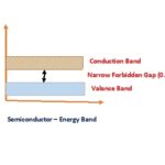
Energy Band
The amount of energy available in electron is depends on orbit of an atom which it configured. The energy levels of electrons within their shell can be caused due to the changes in their energy levels. According to their energy level the band are classified as below,
- Conduction Band
- Valance Band
- Forbidden Gap
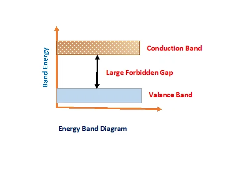
1. Conduction Band
The electron which loosely bind with nucleus can be detached easily and can be shifted to neighboring atom. This electron occupies less amount of energy.
2. Valance Band
The energy level available in outermost orbit is less than inner orbit. It can be brought to conduction band by applying required amount of force.
3. Forbidden Gap
It is gap between valance band and conduction band. There is no electron movement in this gap. But to bring electrons from valance band to conduction band through this band only. The Forbidden gap measured in eV (Electron volt)
Now Let us study about how energy band diagram available in different materials,
1. Conductor
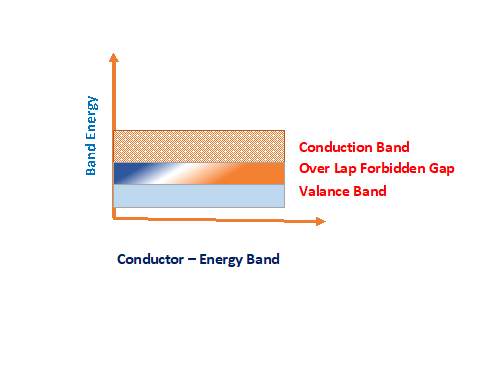
It is named as conductor, because it easily conducts electricity from one end to another end of electrical circuit. A conductor has more free electrons, they are loosely bind with nucleus of an atom. So a small amount of electro motive force is enough to detach their electrons from its nucleus. The energy band diagram shows their valance band and conduction band are overlapped. Hence it offers ample quantity of free electrons. So a very small force can drift these electrons in a certain direction
2. Insulator
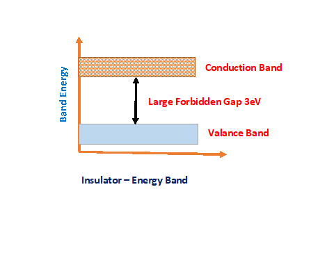
Insulator are never conduct electricity, because there is no free electron are available. All electrons are rigidly bind with nucleus of an atom. Energy Band diagram shows There is large gap between valance band and conduction band. Further it clearly indicates that almost no free electrons are available to conduction band. So to bring electrons to conduction band very large amount of force to be applied. This force will be almost failure of insulator properties which cannot be retained gain. Forbidden gap for insulator around 3eV
3. Semiconductor
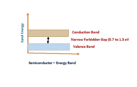
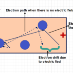
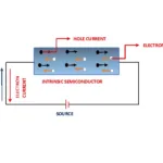
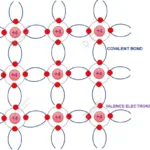
Semiconductor conductivity are in between state of conductor and insulator. During room temperature it act as almost insulator. While increase of temperature, it increases free electrons. Hence act as conductor. Energy Band diagram shows there is a narrow gap between valance band and conduction band. Hence electron drifts to conduction band due to small amount of force applied or a minimal increase of temperature. Forbidden gap for semiconductor about 0.7 to 1.3 eV.
Related posts for you:
 Semiconductor an Overview
 Effect of the Heat and Light while movement of electrons in semiconductor
 Conductivity in the Semiconductor
 Semiconductors Questions and Answers Part-I
 Intrinsic Semiconductor
 Semiconductor Materials
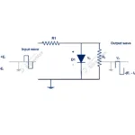
 Series Clipping circuits
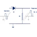
 Shunt Clipping Circuits
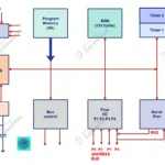 The detailed explanation of 8051 microcontroller block diagram
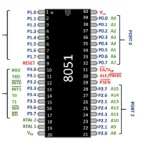 Pin diagram of 8051 microcontroller