Introduction
This article has written about pin diagram of 8051 microcontroller. The microcontroller 8051 is mostly used in educational purposes in colleges and universities for doing small to medium level project works. In addition to , it is used in industrial also to build automation components. However, 8051 is most important and fundamental microcontroller , that every engineer needs to study it in detail.
Pin diagram of 8051 microcontroller
The pin diagram of 8051 microcontroller gives information about input and output ports, interrupts, serial ports etc. about microcontroller. So, it will be useful to configure it perfectly in any kind of circuit to be build. The 8051 microcontroller has 40 pin to communicate with external machines and interfaces. Each pin has its unique functions. The pin diagram of 8051 microcontroller given below.
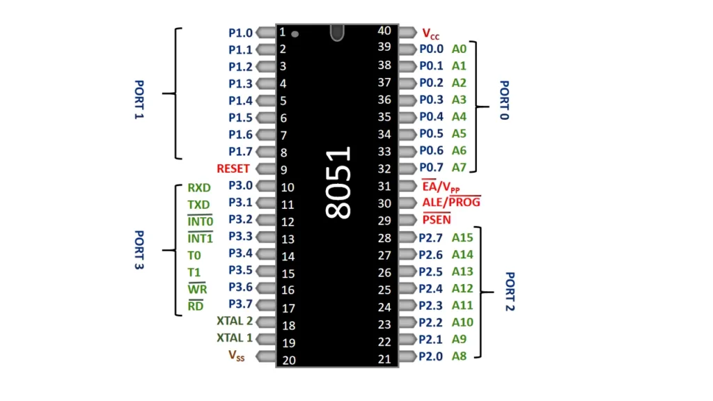
There are four group (P0, P1, P2,P3) of input output port available. Each group made with 8 pins. Moreover, separate pins are provided to give operating voltages etc. The pin details of 8051 microcontroller are explained here,
Pin description of 8051 microcontroller
Port 0 (Pin No : 31 to Pin No: 39)
Port 0 is an 8-bit port . it can be used as both input and output ports. It is also working as bi directional low order address bus as well as data bus to connect with external memory system. The port 0 pin are in open drain configuration mode. So, to connect with external memory system , pull up resistor must be connected with each pin. With pull up resistor connected , to use port 0 as input port , the port must be programmed by writing all bits as 1. Port 0 is also used as lower order address bus from Address bit 0 (AD0) to address bit 7(AD7).
By connecting external memory port 0 can be used both address bus and data bus. These 8051 microcontroller multiplexes address and data through port 0 (pin no:31 to pin no:39) to save pins.
Port 1 (Pin No : 1 to Pin No: 8)
Port 1 can be used common8 bit input and output port. It does not need any external pull up resistor. Because it is internally fabricated. When reset signal occurs in microcontroller port 1 becomes input port. To make port 1 as output port all pins in port 1 must be programmed to write 1 in its all bits.
Port 2 (Pin No : 21 to Pin No: 28)
Port 2 also can be used as common 8-bit input and output port. Further port 2 does not need any pull up resistor. Because it is fabricated internally. Port 2 become input port upon reset of microcontroller.in order to use port 2 as output port , this port must be programmed by writing 1 to its all bits. Moreover port 2 is one more function , that it operates as higher order address bus (AD 08 to AD15). So, it is clearly indicating that port 0 can be used 8-bit data bus as well as address bus. In combination of port 0 and port 2 a 16-bit address bus used to communicate with external memory devices. When external memory connected with microcontroller , port 2 is used as address bus only. It cannot be used as data bus.
Port 3 (Pin No : 10 to Pin No: 17)
Port 3 can be used common input and output port. It does not need any pull up resistor, because it is fabricated internally. Port 3 will be configured as input port upon reset signal occurs in microcontroller. Port 3 also having some alternate function , those are most useful to operation of microcontroller and practical applications.
| Pin ID | Pin Description | Alternate Function |
|---|---|---|
| P3.0 | RXD | Serial input line to receive communication data |
| P3.1 | TXD | Serial output line to send communication data |
| P3.2 | INT0 | External interrupt input 0 |
| P3.3 | INT1 | External interrupt input 1 |
| P3.4 | T0 | External timer 0 input |
| P3.5 | T1 | External timer 0 input |
| P3.6 | WR | External data memory write strobe |
| P3.7 | RD | External data memory read strobe |
RESET (Pin No:9)
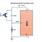
Reset pin is active high input to reset microcontroller. Ton reset microcontroller , at least high pulse to be maintained up to two machine cycle. This reset called as power ON reset. After reset microcontroller all content stored in registers of microcontroller will be cleared. Microcontroller will become default mode.
ALE/PROG (Pin No:30)
It is active high input pin. ALE expressed as address latch enable. It used to de-multiplex address and data bus in port 0. Because port 0 can be used both address and data bus. ALE pin used for de-multiplexing data and address bit by connecting 74LS373 latch. Same pin also used to give program pulse input during EPROM programming.
PSEN (Pin No:29)
This pin expressed as program store enable. This is an output pin connected with OE pin of the ROM. When 8051 microcontroller fetching memory from internal memory PSEN will be high I.e. deactivated. When microcontroller fetching memory from external memory , PSEN will be low twice in each machine cycle., except that PSEN activation are skipped during each access of external data memory system.
EA/Vpp (Pin No: 31)
The EA pin needs to be connected with VSS (ground) to enable microcontroller to fetch code from external memory from locations starting from 0000H to FFFFH.
On other hand EA need to connected with Vcc , to fetch code from internal memory.
There is alternate function in this pin which is Vpp. This pin connected with 12.75 voltage, which should be used programming supply voltage during EPROM programming.
XTAL-1 (Pin No:19)
This pin used as input pin to the inverting oscillator amplifier and internal clock generating circuits.
XTAL-2 (Pin No:18)
The pin used as output pin to the inverting oscillator amplifier.
VSS (Pin No:20)
It is used to connect 8051 microcontrollers with common ground to input supply voltage.
VCC (Pin No: 40)
This pin used to connect 8051 microcontroller to +5V dc supply to provide operating voltage to its internal circuits.
For further details of internal circuits read block diagram of 8051 microcontroller

